Antimonene is predicted to have interesting properties that would make it suitable for optoelectronic devices
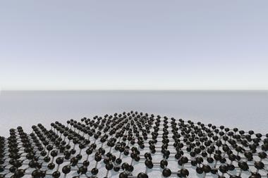
The monolayer materials family has welcomed its newest member: antimonene. The new material is an atom thick layer of antimony and is predicted to have extraordinary electronic properties.
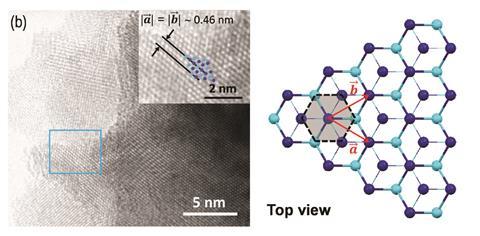
Antimony crystals have a layered structure much like that of graphite. To produce antimonene, the Spanish team used a mechanical exfoliation method similar to the one that was first used to make graphene from graphite – using pieces of tape to peel off the material one layer at a time. Normally the thin layers of the exfoliated 2D material are transferred to a piece of silica, but this didn’t work well for antimonene. Instead, researchers developed a new procedure to transfer the monolayer to a softer substrate: a viscoelastic polymer. This allowed them to obtain bigger antimonene flakes in a more controlled way. Transmission electron microscopy proved monolayers existed, and atomic force microscopy (AFM) techniques allowed scientists to measure their thickness: 0.4 nm.
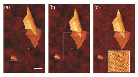
Antimonene may have some very interesting electronic properties when compared with graphene and 2D transition metal dichalcogenides (TMDCs). Graphene uses as a semiconductor have been limited as it has no band gap. By contrast, band gaps for TMDCs range between 1.5 and 2.5eV, making them too large for certain optoelectronic applications. The predicted electronic properties of antimonene are around 1.2eV, making them ideal for optoelectronics. The only monolayer material with similar electronic properties is phosphorene, synthesised just two years ago. But phosphorene is derived from black phosphorus, and so is highly hygroscopic and reactive. Antimonene, however, is highly stable and can be immersed in water. It can even be folded up using AFM nanomanipulation, proving the allotrope’s exceptional flexibility and strength.
References
P Ares et al, Adv. Mater., 2016, 28, 6332 (DOI: 10.1002/adma.201602128)







No comments yet