
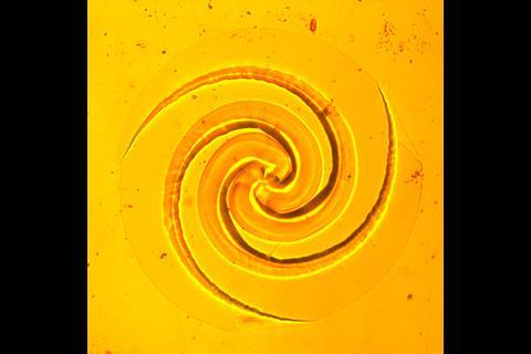
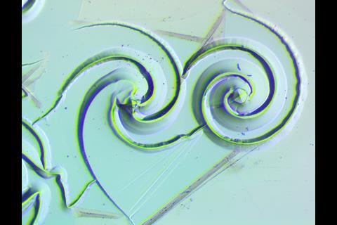
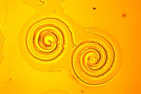
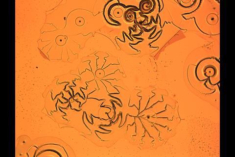
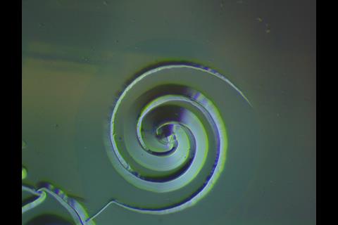
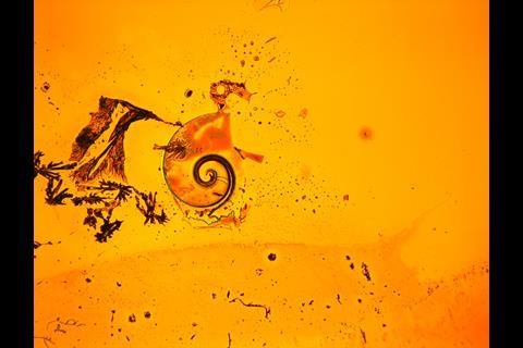
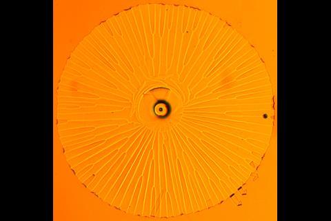
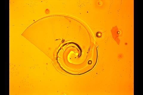
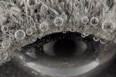
A ‘stunning’ series of microscopic patterns produced by metal-catalysed etching of the surface of a germanium wafer has been captured after a sample was accidentally left out overnight.
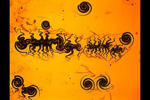
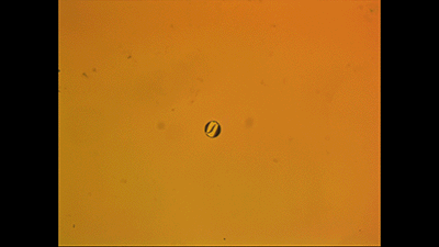
When viewed under a microscope, the tiny dots that had appeared on the sample turned out to be beautiful spirals etched into the surface of the germanium by a chemical reaction.
To understand how the patterns formed, the team of two based at the University of California, Los Angeles investigated a solid-state system that involved evaporating a 10nm thick layer of chromium on the surface of a germanium wafer, followed by a 4nm layer of gold. They then placed a drop of mild etching solution onto the surface and dried it overnight, before washing and re-incubating the chip with the same etching solution in a wet chamber to prevent evaporation.
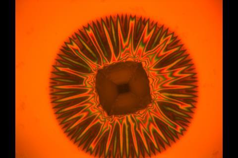
They found that, over a period of 1 to 2 days, a chemical reaction catalysed by the metal film resulted in hundreds of geometrical surface patterns – spirals, radial patterns and more disordered structures – at ∼100μm forming on the germanium.
The patterns were etched onto the germanium surface at the interface with the metal film. During the process they found that the metal films were under stress, resulting in them detaching from the germanium’s surface. Some of the etching patterns seen were associated with Euler buckling of the metal layer, following its detachment.
Small changes to the experiment, such as altering the thickness of the metal film or the initial state of mechanical stress of the sample, were found to influence the resulting patterns.
References
Y Wong and G Zocchi, Phys. Rev. Mat., 2025, 9, 035201 (DOI: 10.1103/PhysRevMaterials.9.035201)


No comments yet