Higher quality material produces largest band gap ever recorded
Scientists in the US and France have produced graphene with a record high band gap of half an electronvolt (0.5 eV), which they claim is sufficient to produce useful graphene transistors. The band gap owes itself to highly periodic bonding on a silicon carbide substrate.
![]()
Graphene, a single layer of carbon atoms arranged in a honeycomb-shaped lattice, exhibits a range of superlative properties. Since it was discovered in 2003, it has been found to have exceptional strength, thermal conductivity and electric conductivity. The last property makes the material ideal for the tiny contacts in electronic circuits, but ideally it would also make up the components – particularly transistors – themselves.
To do so, graphene would need to behave not just as a conductor but as a semiconductor, which is the key to the on–off switching operations performed by electronic components. Semiconductors are defined by their band gap: the energy required to excite an electron stuck in the valence band, where it cannot conduct electricity, to the conduction band, where it can. The band gap needs to be large enough so that there is a clear contrast between a transistor’s on and off states, and so that it can process information without generating errors.
Regular graphene has no band gap – its unusually rippled valence and conduction bands actually meet in places, making it more like a metal. Nonetheless, scientists have tried to tease them apart. By fabricating graphene in odd shapes, such as ribbons, band gaps up to 100 meV have been realised, but these are considered too small for electronics.
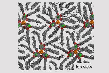
Edward Conrad at the Georgia Institute of Technology, US, and colleagues fabricated their graphene by epitaxial growth. In this method, a silicon carbide (SiC) substrate is heated to temperatures of 1360°C, at which point it begins to decompose and form graphene layers. The researchers found that the first of these layers, normally called the buffer layer, forms a band gap greater than 0.5 eV, because of the highly periodic way it bonds to the SiC substrate.
Guido Burkard, a physicist at the University of Konstanz in Germany who was not involved in the work, says this is ‘almost, but not quite’ as large as the band gap in regular semiconductors. ‘It remains to be seen whether the graphene produced in this way also possesses the favourable electronic properties of previously studied graphene samples,’ he adds, ‘but the result reported is certainly very promising.’
Conrad and colleagues’ epitaxial method for generating semiconducting graphene is not new. In 2006, a group led by Alessandra Lanzara at the University of California in Berkeley, US, investigated the second layer of graphene grown epitaxially above silicon carbine, and reported a band gap of 0.26 eV. Conrad says the main difference in his group’s work is the honing of the growth technique. ‘It turns out that crystalline order is extremely important to get this band gap, and they didn’t have that,’ he explains.
When Conrad and colleagues tried growing their graphene just 20°C lower than their favoured temperature, they found that the band gap was non-existent. Conrad likens the development to the early days of silicon electronics. ‘If you go back to the early days of silicon transistors in the 1960s, it was really about [finding] incredibly highly ordered crystals,’ he says. And the high cost of silicon-carbide wafers doesn’t matter at this stage, he adds. ‘The first [silicon] transistors they sold were $1,500. The point is, you get the device first, and you worry about the cost later.’
Conrad claims that his colleagues at Georgia Tech are already using his semiconducting graphene to make transistors, with on–off current ratios on the order of one million to one – ten times more than is required by regular electronics. ‘So, it’s starting to work,’ he says.
References
M S Nevius et al, Phys. Rev. Lett., 115, 136802 (DOI: 10.1103/PhysRevLett.115.136802)


No comments yet