
A new way to create ultra-thin layers of metals makes it possible for scientists to study a new and unusual class of 2D materials. Researchers in China used the technique to make layers of five different metals that were only a few angstroms thick, uncovering exotic physical properties.
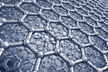
Recent years have seen an explosion of interest in 2D materials. These single-layered structures, like the ‘wonder material’ graphene, tend to display unusual electronic properties, making them highly sought after for a range of different applications.
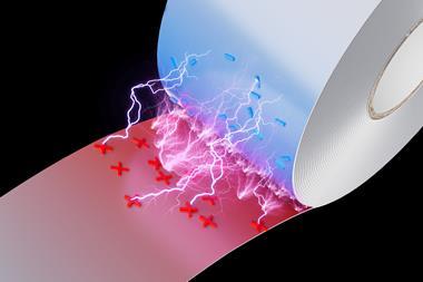
Most of the 2D materials that have so far been investigated fall into a category known as van der Waals-layered materials. These are made from layered crystalline materials in which the interactions between different layers are very weak. This weak bonding makes it relatively easy to isolate single layers by using techniques like mechanical exfoliation, as seen in the famous Scotch tape method used to discover graphene.
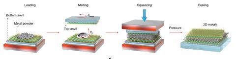
Because metals form strong bonds in all directions, it is much more difficult to isolate just a single layer of a metallic structure. Now, a team led by Beijing-based Luojun Du and Guangyu Zhang has developed a technique to reliably produce angstrom-scale layers of a range of non-van der Waals materials.
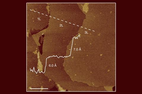
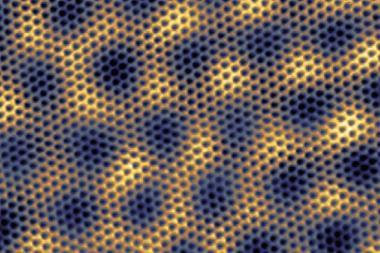
The team’s approach involves squeezing a molten layer of metal between two molybdenum sulfide-coated sapphire anvils at high pressures. The anvils are then peeled away, leaving the thin metal layers encased between the molybdenum sulfide monolayers, which protect the sample from the surrounding environment. The team used the technique to create samples of tin, bismuth, lead, indium and gallium, ranging from 5.8Å thick for tin to 9.2Å for gallium.
The 6.3Å-thick bismuth sample is just two atoms deep and was stable for a whole year while the team tested its properties. The researchers noted that the bismuth sample shows strongly enhanced electrical conductivity, a notable field effect and a new and ‘prominent’ phonon mode.
The team notes that the ‘universal’ method could enable the ‘investigation of emerging quantum, electronic and photonic phenomena’ for a diverse range of materials.
References
J Zhao et al, Nature, 2025, DOI: 10.1038/s41586-025-08711-x


No comments yet