Two studies reveal how radiation damages materials at the nanoscale
Two studies have provided new insight into how radiation causes nano-scale defects in materials - changing their properties dramatically or leading to dangerous cracks that weaken them. The research has implications ranging from nuclear power generation to the design of future nanomaterials.

Radiation can have detrimental effects on materials - damaging components in nuclear reactors, for example. But it can also be useful in techniques such as ion implantation, which uses radiation to produce different types of silicon semiconductor for microchips.
When exposed to radiation, atoms in a crystalline metal structure can be knocked out of their original position (leaving a ’vacancy’) and take up position where there would normally be a gap in the lattice - a so called ’interstitial’ defect. Often, the crystalline lattice rearranges to minimise the effects of the defects on the structure by positioning them all together. This creates tiny disc-shaped bumps or ’dislocation loops’ comprised of hundreds of defects.
Steven Zinkle, who worked on the project at the University of Tennessee, US, told Chemistry World: ’We have discovered a very efficient migration mode for transporting these groups of vacancies. What makes this research surprising is that this happens with energies that are well below what it would normally take to transport a single vacancy.’
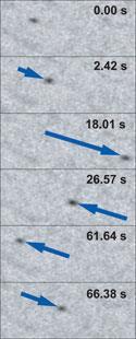
A second team of scientists at Osaka University in Japan identified how the nanometre-sized dislocation loops can rapidly move in a single direction through the lattice structure of iron without any external forces being applied.
Brian Wirth, a professor of nuclear engineering at the University of California, Berkeley, US, explained to Chemistry World: ’The fact that the defects can migrate (and bring along solutes or impurities) may provide the ability to precisely deliver regions of solute enrichment where required.’
Wirth added that defects could be removed or even arranged to form patterned nanostructures. ’Such materials could have unique electronic and optical properties due to the patterning.’
Lewis Brindley
References
Scienceet alScience, 2007; DOI: 10.1126/science.1145386


No comments yet