
Centuries of study have refined theories of how substances with periodically ordered structures behave. Anna Demming talks to the researchers exploring where these theories can apply in materials that are not ordered periodically, or even ordered at all
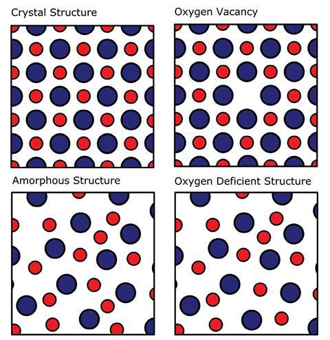
‘Defects’ are the main bugbear in the amorphous materials used as dielectrics in microelectronics – an industry that gives these materials a sharply rising global market value of $66 billion (£51 billion) as estimated in 2023. Yet to what extent these ‘defects’ actually resemble the crystal features from which they get their name remains a point of debate. In the literature on crystals, a ‘defect’ is any feature that breaks the regular order of the repeating crystal lattice – from sites on the crystal lattice with different chemical species swapped in, to sites where atoms are absent altogether. However, amorphous materials have no long-range repeating periodicity.
These gaps in our understanding of amorphous dielectric materials have persisted despite assiduous research over the past 50-year boom in the semiconductor industry. The theory of amorphous dielectrics borrows a lot from the physics of crystals with little clarity as to how valid these ideas may be when where there is no long-range order. And they are not the only materials where concepts from crystallography are applied even though the arrangement of atoms does not follow the periodic order of a regular crystal. Quasicrystals are now not only widely accepted among the scientific community, but accepted as ‘crystals’ thanks to a redefinition of the term by the International Union of Crystallography in 1992.
Recent research is now beginning to clarify what sort of behaviour we can expect from amorphous materials and quasicrystals, and just when and why theories developed for regular crystals can apply. Furthermore the discovery of a single shape that can tessellate to infinity without gaps or repeats in the pattern has prompted investigations of what the material properties of such a structure might be, unearthing a new playground somewhere between the crystalline and quasicrystalline world.
Order absence
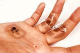
Amorphous materials offer much cheaper dielectrics for microelectronics, since they obviate the high temperatures needed for crystallisation. It is also easier to make them less brittle, which is useful for increasingly popular flexible and wearable electronics. According to Jack Strand of University College London, UK, the crystals used in microelectronics are usually polycrystalline, so that grain boundaries introduce a ‘reliability problem’, which is expected to improve in amorphous materials where they are absent. But while the lack of long-range order seems to give amorphous materials immunity to grain boundaries, this does not seem to apply when it comes to defects.
The challenge of characterising these amorphous materials is partly responsible for the difficulty pinning down what is going on when ‘defects’ occur. They are often produced as thin films just nanometres thick, which makes it difficult to apply standard crystallography techniques like x-ray diffraction. Furthermore, the lack of order in these materials, not just in the way atoms are arranged but also the strength of interactions between them, complicates efforts to describe what is going on.
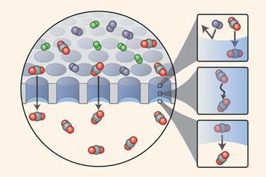
Silicon dioxide (SiO2) offers one of the simpler examples of how parallels with crystal defects can be drawn and is also one of the most popular dielectrics in microelectronics on account of its properties and the ease of integrating it with silicon devices. Crystalline SiO2 is prone to oxygen vacancies where a lattice site that should be occupied by oxygen is empty. Although the atoms in amorphous SiO2 are randomly positioned, each silicon is bonded to four oxygen atoms and each oxygen to two of silicon. As in crystalline SiO2, an oxygen atom may be missing, leaving a ‘vacancy’ behind that is evident from the two silicon atoms that are only bonded to three oxygens. Just like defects in a crystal, these oxygen vacancies can be thought of as point defects that can move around and aggregate, creating vacancy-rich regions with more metallic behaviour that can lead to dielectric breakdown. However, researchers are also identifying ways in which the characteristics of defects in crystals and amorphous materials diverge.
Calculations have shown that in amorphous materials defects can be hard to keep track of. The meaning of a ‘site’ is less defined in amorphous structures than in crystalline ones. Computational studies that calculate the arrangement of atoms using parameters from experiment suggest that if you remove an atom and raise the energy (temperature) of the system so that it relaxes, the site of missing oxygen can no longer be located. ‘It’s almost like it’s been smeared out and assimilated into the system,’ says Strand. ‘I don’t think I’ve ever seen anything like this being reported for crystals.’
Things also get more complicated with materials like hafnium oxide – which has a higher dielectric constant than SiO2, and so is particularly useful for high-power electronics – and aluminium oxide. Here the number of oxygen atoms each metal atom bonds to is more distributed. For example, 40% of the metal atoms might be bonded to four oxygen atoms, 40% to five and 20% to six. In that scenario an absent oxygen atom is a lot more difficult to identify. The strength of the bonds are also distributed probabilistically. Nonetheless these oxides are also prone to breakdown in ways that inculpate oxygen deficiencies. Strand, together with UCL colleague Alexander Shluger and coworkers, has identified some of the critical physical processes involved in oxide degradation.
Despite gaps in our understanding, engineers have figured out work arounds that improve the dielectric performance of oxygen deficient amorphous oxides. Heating up an oxide in hydrogen is a popular way of ‘passivating’ defects in amorphous oxides, which makes them far more valuable to the microelectronics industry. A better grasp of the theory could reveal the potential for alternative gases such as nitrogen, which Strand is currently investigating. Although nitridation of hafnium oxide is common practice, the mechanisms at play are not well understood. To complicate the issue, overexposure to elements like hydrogen can start to reverse the process as the hydrogen prefers to form molecules with other hydrogen atoms instead. ‘So theoreticians try to understand, if there is some success, why this is happening,’ says Shluger, explaining how theory can help chemical engineering with defects.
Engineering aperiodic materials
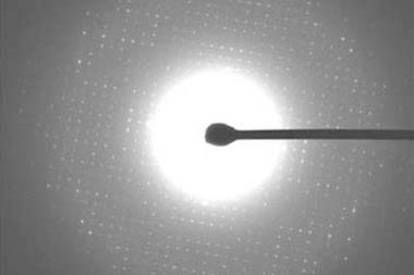
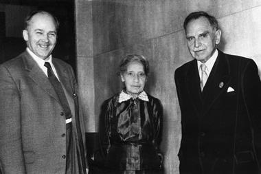
While defect engineering in amorphous materials attempts to fine-tune properties when the position of the atoms is random, elsewhere theoreticians are looking at what happens to the properties of materials when the positions of the atoms are regulated although not within a repeating pattern. Quasicrystals are defined by a long-range order that lacks translational periodicity. That means it is possible for them to have types of rotational symmetry that had been considered ‘forbidden’. ‘When you’re an undergraduate, you learn this thing called the crystallographic restrictions theorem,’ says Felix Flicker, a theoretical physicist at the University of Bristol in the UK. ‘It says that crystals can only have two-, three-, four-, or sixfold rotational symmetries.’ For example, you can rotate a square grid by 90 or 180° and the grid corners or vertices lie exactly where there were vertices before the rotation. For a regular triangular grid rotation, 120° would render the same pattern, but there are no periodic grids that are symmetric under a revolution by 72° or fractions of 360° smaller than a sixth. The same crystallographic restrictions apply in reciprocal space when looking at the diffraction patterns of x-rays incident on a sample of the material. However in 1982 Dan Shechtman and his colleagues studied a rapidly cooled sample of aluminium manganese and concluded from the Bragg diffraction pattern that it had five-fold symmetry, describing it as a ‘quasicrystal’.
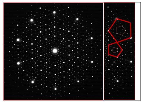
At that time the crystallographic restrictions were so entrenched that a lot of people thought they had just got it wrong. ‘There is no such thing as quasicrystals,’ said leading chemist and twice Nobel laureate Linus Pauling; ‘only quasi-scientists.’ Indexing quasicrystals introduces more complications. While people would normally only need one integer per dimension to index the diffraction pattern, which would pin down the unit cell, quasicrystals need five or six indices. Nonetheless the evidence for quasicrystals ultimately stacked up in Shechtman’s favour and he received the 2011 Nobel prize for chemistry for their discovery.
Meanwhile steady developments in maths have unearthed a whole host of aperiodic patterns that have long-range order but never repeat, and ways of creating them. One is to twist the orientation of two regular hexagonal lattice grids by exactly 30° with respect to each other, as reported by Peter Stampfli in 1986. In 2018, this structure was produced in carefully grown bilayer graphene (two layers of carbon atoms that arrange in a hexagonal lattice) by a team of researchers in South Korea, the US and Japan. Experiments with graphene have also yielded an aperiodic structure by another route: overlaying two periodic lattices where the ratio of the units of periodicity for the two lattices is an irrational number. The combined mesh of twisted layers of graphene gives the effect of a moiré lattice with a larger lattice constant, like the double meshed fabrics they take their name from. In 2023, researchers led by Pablo Jarillo-Herrero at Massachusetts Institute of Technology in the US experimenting with trilayer graphene managed to (accidentally, as one of the researchers on the team, MIT’s Aviram Uri, told Chemistry World at the time) produce two moiré lattices with an irrational number lattice constant ratio.
One of the questions around the structures created by layering graphene is whether they are really quasicrystals or just incommensurate crystals; that is, whether they ultimately just break down into two regular crystals each with its finite unit cell length, which is not possible for the quasicrystals Schechtman discovered. Although these structures are created from layering regular lattices, strong interactions between the layers (which can be identified through angle-resolved photoemission spectroscopy, ARPES, as later reports have also highlighted) suggest descriptions of the whole system as two distinct crystals layered on top of each other is no longer valid.
Quasicrystals may prove particularly useful in areas such as catalysis
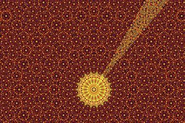
Certain properties become much more interesting in the case of quasicrystals, such as the connection to higher dimensions. As Flicker explains, what appears to be an aperiodic pattern in one dimension could be produced by taking a slice through a regular 2D pattern where the slope length is described by an irrational number of unit cells, and then projecting the points into one dimension. The additional indices needed to describe the diffraction patterns can be considered a trace of these higher dimensions, and quasicrystals can take on topological properties in higher dimensions too. Although an incommensurate crystal made from two 2D crystals could be described as sort of 4D, ‘because they’re totally disconnected from each other, no one really buys that as a 4D structure’, Flicker tells Chemistry World. ‘Whereas in the quasicrystal, it’s just like one pattern in two dimensions, which is not a periodic one, and that itself has this sort of knowledge of this four-dimensional space.’
As well as intriguing from a fundamental science point of view, Flicker suggests quasicrystals may prove particularly useful in areas such as catalysis. Alongside Shobhna Singh at Cardiff University in the UK and Jerome Lloyd at the University of Geneva in Switzerland, Flicker has recently shown a way of tracing a path through aperiodic patterns that visits each vertex exactly once. This translates to a way of optimising coverage when adsorbing molecules as in catalysis. ‘So it means that bendy molecules can pack onto these quasicrystals perfectly, which wasn’t obvious at all,’ adds Flicker. It also offers a way of exploring how proteins may fold, and here the aperiodic lattice provides an advantage over lattices with a regular period because more realistic geometries can be explored.
Although periodic lattices had been easier to solve for these paths, Flicker and colleagues identified a mathematical property known as ‘perfect dimer matching’ in a particular type of aperiodic pattern made from two tile shapes – Ammann–Beenker tilings. Dimer matching can be thought of as a puzzle where the aim is to highlight edges – lines joining the vertices – so that every vertex touches one and only one highlighted edge, which is not always possible. For instance Penrose tilings were the first aperiodic patterns to be pinned down and it was soon shown that they can also be created from just two tile shapes too, but they do not allow perfect dimer matching.
The hat
For several decades after the discovery of Penrose tilings, the hunt was on for a single shape that could tessellate aperiodically. In November 2022, a retired print technician in the Yorkshire seaside town of Bridlington discovered ‘the hat’, which seemed to fit the bill, and this was later confirmed with tremendous excitement by mathematicians.
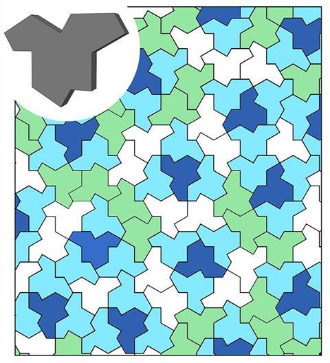
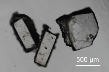
‘I was fascinated by the elegant design and thought that the simplicity of using a single tile could impact various areas of research,’ says Grace Gu, a mechanical engineer at the University of California in Berkeley, US. Intrigued by the possibilities, she and her group created polymer composites with aperiodic structures of tessellated hat tiles, where each tile is around 5mm across, outlined in a softer polymer boundary material. Composites are useful for harnessing the beneficial properties of two different materials, such as toughness and strength. However, they are usually assembled with a periodic structure, which is vulnerable to fault lines where catastrophic failure can propagate. The aperiodic monotile provides a way of avoiding such vulnerabilities along with the advantages of long-range order.
Gu and her colleagues compared the aperiodic monotile structured composite with a regular hexagonal composite structure made with the same materials and sample sizes and found that the aperiodic composite outperformed its regular counterpart in terms of stiffness, strength and toughness. ‘The way the tiles interacted with their neighbouring tiles, and the absence of gaps between them, resulted in better stress transfer,’ says Gu, who puts the material’s success down partly to the excellent interlocking between the tiles. She expects that making the composites with smaller tile shapes may improve the properties because of the higher surface area for interlocking, which they are looking into experimentally. But there’s a limit, she adds: if the tile size gets too small it may effectively ‘behave like a homogeneous material’. Homogenous amorphous materials are engineered for strength too using alloys but Gu expects comparisons of composites exploiting hat-shaped structures to compare favourably with amorphous alloys too, although again experiments with those kinds of metals are yet to be performed.
To put an extra atom onto a quasicrystal, it needs to know where all the other atoms in the quasicrystal are
There is a point at which decreasing the size of the hat-shaped tiling may introduce material properties that are interesting in other ways. Flicker has been calculating the kind of properties that might come from a crystal with an aperiodic monotile microstructure and comparing them with regular crystals like graphene. He highlights that some of their properties seem to stem from the fact that they only have one unit cell – like a crystal, and like graphene in particular – such as the sixfold symmetry and certain electronic features. This can be understood since the ‘hat’ shape can be thought of as an inspired derivative of tessellated hexagons. ‘So in a sense, you’ve started from a crystal and sort of weakened the couplings on a select set of the sites and turned it into a quasicrystal,’ says Flicker. Conversely his work also highlights other properties that come from the fact that the unit cell doesn’t repeat periodically, such as the presence of zero energy modes in the electron wave function. ‘These monotile things are kind of between crystals and quasicrystals, that’s how I would see it.’
So far crystals with aperiodic hat microstructures are yet to be realised. However crystals with other aperiodic structures such as Penrose tiling have been grown up to millimetres sizes, which amounts to the self-assembly of around 1023 atoms – how remains a mystery. For a regular crystal, each atom just positions itself so as to minimise its free energy with respect to the atoms nearby. ‘But with a quasicrystal, that’s not true,’ says Flicker, highlighting that attempts to put together a Penrose tiling pattern by eye instead of by following the mathematical theorem that defines them can get to a size of 10,000 atoms before it becomes clear that the whole thing is wrong. ‘To put an extra atom onto a quasicrystal, it needs to know where all the other atoms in the quasicrystal are.’
One suggestion is that something like an aperiodic structure forms with lots of defects in it, and this stabilises and adjusts over time. For all the differences between amorphous materials and quasicrystals, and the diverging problems research in these areas aim to solve, it is possible that defect engineering may play a role not just in crystals and amorphous materials but in producing high quality quasicrystals too.
Anna Demming is a science writer based in Bristol, UK


No comments yet