Extremely low-loss, chemically stable perovskite nanowires have been produced using simple solution deposition.1 The technique can produce optically active waveguides and could, therefore, allow the scalable production of cheap, miniature lasers for sensing applications.
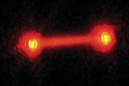
Lead halide perovskites are often seen as a promising material for photovoltaics as their direct bandgaps make them more optically absorbent than silicon and they can be tuned by altering the specific cations and anions in the lattice. Moreover, perovskites can be deposited directly from solution. In principle, they should also make excellent LEDs and semiconductor lasers.
Perovskite lasers were first demonstrated over 10 years ago, when researchers Song Jin at the University of Wisconsin, Madison in the US and colleagues discovered how to turn 3D-perovskite structures into nanowires.2 Three-dimensional perovskites face serious stability issues, however, as ions tend to migrate within the lattice. Two-dimensional organic–inorganic perovskites are inherently more stable – a 2D ‘passivation’ layer is often grown on the surface of perovskite photovoltaics to help stabilise them.
In the new work, the researchers produced nanowires of 2D perovskite by molecular templating. ‘It was kind of an accidental discovery,’ says Letian Dou of Purdue University in Indiana. ‘A major part of my group’s effort is to design new cations to assemble them into 2D perovskites. In the past we’ve made a lot of conjugated structures that made the perovskite very stable.’ The researchers used an organic cation that formed regular bonds to sites in the inorganic layer of the perovskite, creating a hydrogen-bonded network of parallel nanowires on the substrate, while suppressing growth in other directions.
The hydrogen-bonded network was actually too strong to excise nanowires, however. The researchers found that crystal defects were present and suspected that these were due to strain in the inorganic lattice. They therefore replaced the organic cation with another one, which allowed for some breaks in the hydrogen-bonded chain. This produced pristine nanowires that, they showed, produced very low-threshold lasers whose bandgaps could be tuned by altering the other ions.
‘There’s a lot of need for low-cost lasers for sensors, Lidar, the internet of things,’ says Dou. At present, such miniature lasers are feasible only using semiconductor devices such as gallium arsenide, which use more expensive materials and have to be fabricated using complex techniques such as chemical vapour deposition or molecular beam epitaxy.
Jin is impressed by the researchers’ creation of nanowires from 2D perovskite. His own group, he says, wanted to achieve this for many years but couldn’t do it. He cautions that the specific technique used here, which relies on tailoring the organic ligand so that it anchors to a precise point on the inorganic layer, could prevent its applicability to other perovskites with desired photophysical properties. Nevertheless, he says, the increasing ability to grow single crystals of perovskites is likely to lead to a renewed interest in the near future in perovskite lasing and concludes that ‘from that point of view, this is a very useful and important development’.
References
1 W Shao et al, Science, 2024, 384, 1000 (DOI: 10.1126/science.adl0920)
2 H Zhu et al, Nat. Mater., 2015, 14, 636 (DOI: 10.1038/nmat4271)






No comments yet