
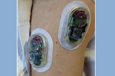
The largest perfect two-dimensional crystals of the insulator hexagonal boron nitride (hBN) and the semiconductor tungsten disulfide have been made by researchers in South Korea. The team that created the 9cm2 wafers hope that, if production can be scaled up, they will find use in next generation electronics. By coupling 2D insulators and semiconductors with the 2D conductor graphene it should be possible to create electronics that are both flexible and thinner than conventional electronics.
Of all graphene’s extraordinary properties, perhaps the most remarkable is its extremely high electronic conductivity. This has led some researchers to believe it could be the future of electronic miniaturisation. Electronics also requires semiconductors and insulators in addition to conductors, however. Fortunately, nature has provided scientists with monolayer versions of these too: some transition metal dichalcogenides are semiconductors and hBN is an insulator. Unfortunately, finding an economical way to produce good graphene is challenging – finding a commercial route to structures comprising several monolayers controllably stacked is even tougher.
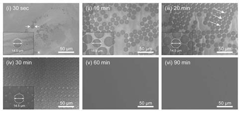
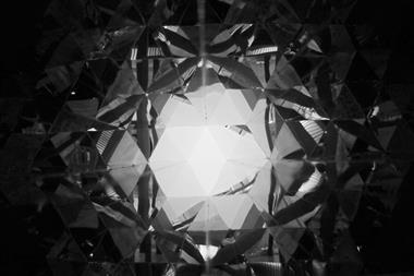
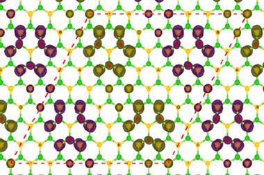
hBN is normally produced by chemical vapour deposition (CVD) of borazine. Unfortunately, 2D crystals of hBN grow with random orientations. When they meet, they form grain boundaries so the sheet has defects making it less useful for electronics. Now researchers at several South Korean institutes have added a neat twist: they perform the CVD at 1100°C on a tungsten substrate covered with gold foil. As the gold melts, the hBN crystals form on a thin film of liquid gold covering the tungsten, leaving them free to rotate. Similar techniques can produce high quality graphene layers, but they are still not perfect single crystals. Unlike graphene, however, boron nitride contains dipoles. As the randomly-oriented crystals join up, the forces between them cause the individual crystals to align and stitch together into one perfect crystal. The expensive gold foils can also be used repeatedly to keep costs down.
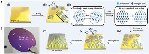
The researchers used their 3cm×3cm wafer – whose size is limited only by the vacuum chamber – as a substrate for CVD to make similarly-sized, single crystal layers of graphene to produce a two-layer heterostructure. ‘You get an electronic mobility improvement in graphene on single crystalline hBN,’ explains Young Hee Lee of the Institute for Basic Science and Sungkyunkwan University, both in South Korea. Graphene needs high electronic mobility to realise its extraordinary theoretical electrical conductivity. They also tried doing the same thing with the semiconductor tungsten disulfide. ‘Accidentally, we etched away the hBN, leaving a single-crystal tungsten disulfide,’ says Lee. ‘That’s still important, but from a device point of view somewhat limited.’ Lee says that they are still working on the ‘holy grail’ of a single crystal semiconductor on hBN. This could allow them to produce a new type of 2D transistor.
Nanoscientist Jiwoong Park at the University of Chicago in the US is impressed. ‘They’ve found a clever way to produce a film with very uniform direction everywhere,’ he says. ‘That, I’d consider an important development. The ways that hBN influence graphene usually only really matter at low temperature, so I’m hesitant to jump in with an obvious application. But you never know – these new capabilities have a way of galvanising people’s creativity.’
References
J S Lee et al, Science, 2018, 362, 817 (DOI: 10.1126/science.aau2132)


No comments yet