Cheap, printable electronics could be used to make smart labels for packaging
Scientists have used electronic inks made of various different two dimensional materials to build thin film transistors using an inkjet printer. Although printed transistors have been demonstrated previously, this is the first time it has been done using multiple ‘nanosheets’ of 2D materials.
Transistors have previously been made from a single nanosheet or a combination of a small number of nanosheets, and their performance outstrips the capabilities of using nanosheet networks – a disordered collection of 2D flakes of material, akin to millions of pieces of card strewn on a floor. Although these networks are electronically inferior, they do have an advantage. They can be used as an electronic ink for printing components simply and cheaply.
‘Most printed devices are based on organic molecules whose performance is limited,’ says Jonathan Coleman, who led the new work at Trinity College Dublin, Ireland. ‘We believe nanosheet network transistors can compete in this area.’
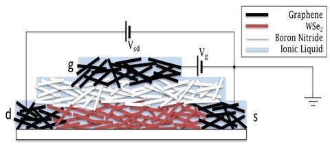
Working with colleagues at other European institutions, Coleman’s lab designed a method of printing nanosheet network transistors onto flexible alumina-coated PET. Each component was made using a different 4D material, creating layers that were then stacked up. Graphene was used for the electrodes, molybdenum disulphide and tungsten selenide for superconducting channels, and boron nitride as the dielectric insulator.
To make the inks the team exfoliated layered crystals using liquid phase exfoliation, a technique developed in Coleman’s lab in 2008. This produces lots of little 2D sheets dispersed in solution, which can then be printed using an inkjet printer. A big challenge, however, was to find a way to switch the current on and off in the nanosheet networks. This has traditionally been difficult because thicker networks are required to get current levels high enough for switching, but also make switching less effective. The researchers came up with an electrochemical workaround, developing a new form of solid electrolyte instead of a traditional dielectric material. This involved filling the pores of the boron nitride network with an ionic liquid, giving a solid-like structure but with ion mobility to accumulate charge and allow switching to occur.

‘This work’s primary accomplishment is the use of an electrolyte in conjunction with the composite nanosheets,’ comments Doug Barlage from the University of Alberta, Canada, who investigates transistor materials. ‘But the application that this has an advantage for isn’t that clear because it is not…as good as known thin film transistors.’
However, Coleman is confident that despite performance limitations, the approach could allow for low cost printed circuitry for applications including smart labels on packaging. ‘The technology is promising but the performance needs to be improved dramatically. We need to increase the mobility, on/off ratio and switching speed,’ he explains. ‘The first will be improved by focusing on improving the inter-nanosheet junctions, the other two properties by optimising the ionic liquid.’
References
A Kelly, et al., Science, 2017, DOI: 10.1126/science.aal4062






No comments yet