Atomic resolution of molecules – warts and all – can help in the development and design of electronics materials
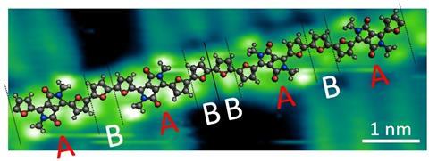
Conjugated polymers have been put under the microscope and imaged in the greatest detail ever. For the first time it has been possible to accurately pick-out structural characteristics of the polymer – including the sequence of the monomers – that give the material its properties. The technique could help to optimise polymer materials for use in flexible lightweight electronics, including organic solar cells, LEDs and sensors.
These polymers are named for their backbone of alternating single and double bonds. This structure is what makes them conductors as they allow an electric charge to move along their chain of monomers. The resulting optical and electronic properties has led to growing interest in them for plastic-based opto-electronic applications.
Let’s deposit polymers on a surface and just look at them
Giovanni Costantini, University of Warwick
However, as more complex polymers are investigated, it becomes harder to control their properties and performance, which are dictated by their microstructure, including monomer sequence and backbone conformation. Current ways to understand their structure rely on molecular modelling or indirect data averages of large numbers of polymers. But these fall short of knowing precisely how structure affects function for a polymer.
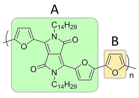
Now, Giovanni Costantini’s group at the University of Warwick and colleagues around the UK have developed an imaging technique that lets them see the structure, including the monomer sequence – defects and all – for the first time. ‘Our guiding principal has been Feynman’s proposal of using high resolution microscopy as the ultimate analytical tool for determining the structure of a chemical substance,’ explains Costantini. ‘The underlying idea is extremely simple yet potentially transformative: instead of using indirect techniques that average over large numbers of polymers, let’s do microscopy of individual polymer strands at the sub-monomer scale; let’s deposit them on a surface and just look at them.’
To achieve this, the team used electrospray vacuum deposition to put individual conjugated polymers onto atomically clean, flat gold surfaces. This provided the necessary conditions to then image individual molecular species using high resolution scanning tunnelling microscopy (STM).
‘The images we have been able to acquire are at such a high spatial resolution that individual monomers can be easily identified and distinguished,’ says Costantini. As a result, the researchers could determine the sequence of monomers that make up the polymer and any defects in the chain by simply looking at the images.
‘This powerful combination of deposition and imaging techniques has the potential to answer important questions associated with the synthesis and organisational principles of conjugated polymers,’ comments Gui Bazan, who investigates organic electronics at the University of California, Santa Barbara, US. ‘One can now identify “mistakes” generated by the polymerisation reaction that lead to structural imperfections. By looking at these errors one can obtain insight into the mechanism of transition metal mediated reactions and the control afforded by different reaction conditions.’
‘The combination of electrospray deposition and STM imaging has worked beautifully for the conjugated polymer studied in this paper and for a number of other conjugated polymers that we have since then studied,’ says Costantini. ‘However, the technique is just in its infancy and we definitively have to further explore its range of applicability,’ he adds.
References
D A Warr et al, Sci. Adv., 2018, 4, eaas9543 (DOI: 10.1126/sciadv.aas9543)








No comments yet